


What is Copper Stamping?

Copper Stamping is designed to meet the modern electrical demands of high-density energy transfer, precise signal switching, and reliability in extreme environments. It is a core element determining the electrical performance and lifespan of critical components such as relays, switches, contactors, and fuses. By integrating precision materials engineering, micron-level forming control, and functional surface treatment technologies, it provides reliable and efficient metal connection solutions for new energy vehicle powertrains, energy storage systems, industrial automation, and smart grids.
Production process of Copper Sheet Metal Stamping Bending Parts
Substrate Pretreatment
The copper strip (0.1- 2.0 mm thick) undergoes degreasing, rust removal, polishing, and annealing to remove surface oxide layers, oil, and impurities. This optimizes surface smoothness and plasticity, improves stamping performance and surface treatment adhesion, and avoids potential problems such as stamping burrs and surface peeling.
01
Precision Stamping
The pretreated copper strip is fixed on a high-precision stamping machine. The pre-calibrated mold is installed, preset stamping parameters are input, and the stamping process is initiated. The blanking gap is controlled at 5%-8% of the material thickness to achieve precise forming of the Electrical Contact Copper Metal Stamping Terminal.
02
Blanking and Finishing
The stamped copper parts undergo precision deburring to remove surface burrs and sharp edges, ensuring a smooth surface and rounded edges. No additional polishing is required, and the parts can be directly assembled. Simultaneously, the dimensions are recalibrated, and Metal Stamping Parts Electric Copper with dimensional deviations exceeding the standard are rejected.
03
Surface treatment
According to customer requirements, products are tin-plated, nickel-plated, or silver-plated, strictly following the specified parameters; the tin plating thickness is controlled at 3-5μm. After completion, a salt spray test (≥72h) is carried out. After the surface treatment is completed, appearance inspection and performance testing are carried out to ensure that there is no peeling, no flaking and no color difference.
04

End-to-End Quality Assurance System of Copper Sheet Stamping for Electric Relay
| Material-Level Control | Each batch of materials undergoes spectral analysis, metallographic examination, and conductivity testing; a material performance database is established to ensure batch-to-batch performance fluctuations are ≤3%. |
| Process-Level Monitoring | A real-time mold condition monitoring system provides early warnings of abnormal wear; closed-loop control of stamping parameters ensures 100% online inspection of critical dimensions; surface treatment thickness and composition analysis is performed, with sampling every 2 hours. |
| Product-Level Validation | Automated Optical Inspection (AOI) system for Electrical Contact Copper Metal Stamping Terminal achieves a 99.9% defect detection rate; functional testing simulates real-world operating conditions, with data stored in the cloud for traceability; accelerated reliability testing includes temperature cycling, vibration, and mixed-gas corrosion testing. |

Packaging and delivery of High Precision Connecting Copper Sheet Metal Stamping
Packaging
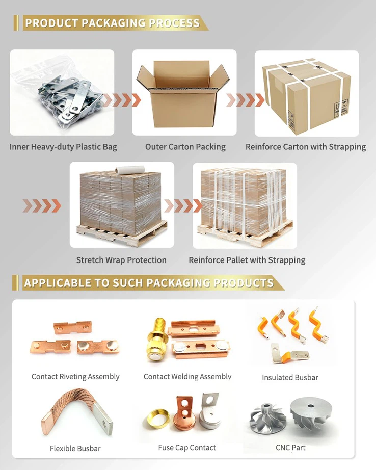
For large and special-sized Copper Spring Contacts, an inner layer of pearl cotton cushioning provides shock absorption and scratch protection; an outer thickened cardboard box with a pallet structure facilitates loading, unloading, and stacking; the outermost layer is covered with a moisture-proof film and reinforced with cable ties to improve transport stability. Before packaging, reasonable layout and size verification are performed, and the outer box is labeled with moisture-proof, pressure-proof, and handling direction instructions.
Express delivery
We partner with multiple domestic and international logistics service providers to develop transportation plans based on the Electrical Contact Copper Metal Stamping Terminal size and weight, and provide full tracking services. We support standard and expedited transportation, as well as palletized and full truckload delivery modes to ensure the safe and timely delivery of large stamping products.
contact us
For technical information, coating solutions, or sample support for Copper Stamping, please contact our engineering team. We will provide you with fast and professional manufacturing assessments and solutions for your project.

Hot Tags: Copper Stamping Parts, Electrical Copper Terminal, Copper Spring Contact, Energy Storage Stamping, Precision Continuous Stamping, Surface Plating Stamping, New Energy Copper Component, Copper Pressed Stamped Parts, copper stamping part, Metal Stamping Parts Electric Copper, Silver Plated Copper Plate, Switch Socket Precision Metal Stamping Parts, metal stamping part


