

Modern high‑voltage electrical distribution systems, EV/HVDC relays, and high‑frequency switching devices demand metal stamped components that maintain strict dimensional stability under severe thermal and mechanical stress. Achieving a dimensional tolerance of ±0.005 mm alongside an electrical conductivity ≥85% IACS requires rigorous control over progressive die design, springback compensation, and micro‑hardness optimization. This engineering guide examines the metallurgical properties, tooling parameters, and quality control protocols required to manufacture high‑performance copper and Beryllium Copper Spring Contacts for global OEM/ODM applications.

Copper Alloy Selection: ≥85% IACS Conductivity and ASTM B152
Material selection determines the allowable stamping load, edge quality, electrical resistance, and post-forming spring behavior.
| Material | Typical Electrical Conductivity | Mechanical Characteristic | Typical Stamping Use |
|---|---|---|---|
| C1100 / C10200 | ≥85% IACS | High ductility | Terminals, busbars, conductive plates |
| C10200 OFHC Copper | ≥100% IACS | High conductivity | Low-resistance electrical components |
| C17200 BeCu | ~22–65% IACS depending on temper | High strength and spring recovery | Contacts, clips, springs |
| C17510 CuBe | Higher conductivity than many BeCu grades | Strength-conductivity balance | Conductive springs and terminals |
Verify copper strip specifications against applicable material standards such as ASTM B152/B194 or the customer's designated equivalent. Also control BeCu by alloy grade and temper, because hardness and spring-back can vary substantially between material conditions.
C1100 Copper Stamping: ≥85% IACS and ±0.02 mm
C1100 copper is commonly selected where electrical conductivity has greater priority than high mechanical strength. The stamping process must prevent excessive burr formation because burr orientation can affect assembly clearance, insulation spacing, and contact geometry.
Typical control points include:
- Conductivity: ≥85% IACS for C1100-type electrical copper.
- Dimensional tolerance: approximately ±0.02 mm for controlled stamped features.
- Burr control: specified by drawing, commonly below 0.05 mm where assembly clearance is limited.
- Material thickness: controlled according to the released engineering drawing.
- Surface condition: free from excessive oxidation, scratches, and stamping cracks.
C17200 Beryllium Copper Stamping: HV and Spring-Back Control
C17200 beryllium copper is selected when a stamped component must combine electrical conductivity with high hardness, elastic recovery, and resistance to repeated mechanical cycling.
After solution treatment and aging, C17200 can achieve substantially higher hardness than commercially pure copper. The exact mechanical values depend on temper, thickness, heat treatment, and supplier specification.
For precision beryllium copper stamping parts, engineering control should include:
- Alloy: C17200 or customer-specified BeCu grade.
- Hardness: controlled according to specified temper, commonly measured by Rockwell or Vickers methods.
- Spring-back: compensated through die geometry and forming sequence.
- Electrical conductivity: verified after heat treatment where conductivity is a design requirement.
- Dimensional stability: checked after forming and thermal treatment.
Consult Our Electrical Engineers Today

Progressive Die Stamping: ±0.02 mm Tolerance and 0.01 mm Clearance Control
High-conductivity metal stamping depends heavily on the relationship between material thickness, punch clearance, die clearance, tool wear, and press stability.
For copper and BeCu strip, excessive clearance can increase burr height and dimensional variation. Insufficient clearance can increase cutting force, accelerate tool wear, and produce secondary deformation around pierced features.
Punch and Die Clearance: 5–15% of Material Thickness
A practical starting range for precision blanking is often expressed as a percentage of material thickness, but the correct value depends on alloy hardness, temper, thickness, tool steel, geometry, and required edge quality.
| Process Variable | Engineering Control | Typical Consideration |
|---|---|---|
| Material thickness | Drawing-controlled | ±0.01–0.03 mm where specified |
| Die clearance | Material-dependent | Often ~5–15% of thickness |
| Dimensional tolerance | Feature-specific | ±0.02 mm typical for selected features |
| Burr height | Drawing-controlled | Often ≤0.05 mm for electrical parts |
| Strip feeding | Servo-controlled | Position repeatability affects pitch |
| Tool wear | Periodic inspection | Directly affects burr and hole size |
For production copper stamping parts OEM programs, tool compensation should be based on actual dimensional measurements rather than a fixed theoretical correction.
Progressive Die Layout: 0.01 mm Feed Accuracy
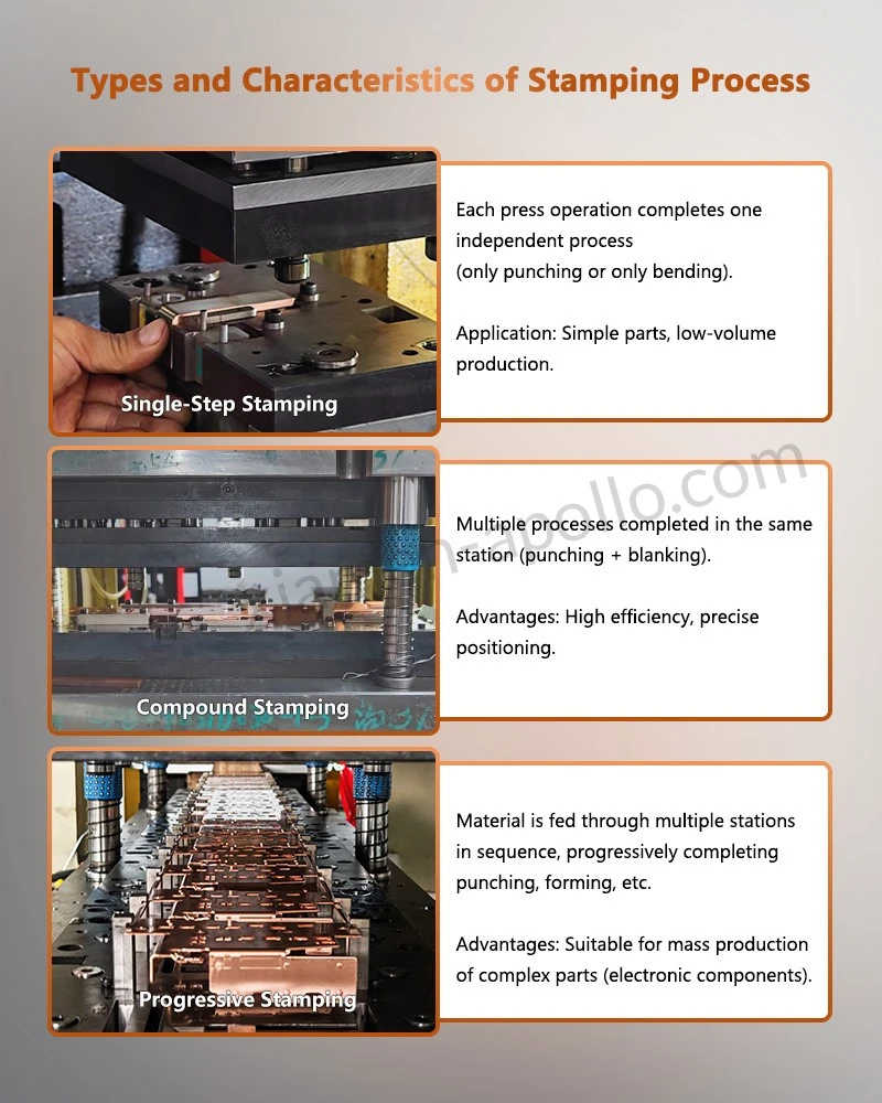
A progressive die can combine blanking, piercing, forming, bending, embossing, and cutoff operations in sequential stations. The layout should minimize unnecessary material movement and maintain consistent strip support around critical features.
Engineering review should consider:
- Strip pitch: controlled according to station geometry and finished-part tolerance.
- Pilot positioning: used to correct cumulative feed variation.
- Punch alignment: monitored to prevent uneven clearance.
- Forming sequence: designed to limit deformation transfer between stations.
- Cutoff geometry: controlled to prevent distortion of functional surfaces.
For miniature electrical terminals, a small change in strip feeding can shift hole-to-edge distance, tab position, or contact alignment enough to create assembly interference.
Burr and Fracture-Zone Control: ≤0.05 mm Edge Requirement
A stamped copper edge normally contains a rollover region, sheared zone, fracture zone, and burr. The proportion of each region changes with material condition and die clearance.
Excessive burr height can increase:
- Electrical creepage and clearance risks.
- Connector insertion force.
- Contact misalignment.
- Plating thickness variation at sharp edges.
- Particle generation during automated assembly.
For parts used in low-voltage electrical equipment, edge requirements should be defined on the engineering drawing rather than left to generic "deburring" language.
In-Die Forming and Riveting: ±0.02 mm Assembly Alignment
Copper and BeCu stamping is frequently combined with secondary operations such as riveting, bending, embossing, welding, and plating. The critical issue is maintaining positional accuracy between the stamped carrier and the secondary feature.
In-Die Riveting: 0.02 mm Contact Position Control
Where a copper or BeCu stamped carrier receives a riveted electrical contact, the rivet hole, carrier plane, and contact axis must remain concentric within the specified assembly tolerance.
Typical inspection points include:
- Rivet-hole diameter: drawing-controlled tolerance.
- Contact position: commonly controlled within ±0.02–0.05 mm.
- Rivet head height: controlled for assembly clearance.
- Joint deformation: inspected to prevent cracks or loose interfaces.
- Contact resistance: verified according to the electrical design requirement.
In-die riveting can reduce separate handling steps, but the die must control both material feeding and rivet positioning.
Resistance Welding: mΩ-Level Contact Resistance
For electrical copper assemblies, resistance welding requires control of current, voltage, electrode force, weld time, and material surface condition.
| Variable | Effect on Joint |
|---|---|
| Welding current | Determines heat generation |
| Electrode force | Controls contact area and resistance |
| Weld time | Influences heat input and nugget formation |
| Surface oxide | Can increase electrical resistance |
| Copper thickness | Changes current distribution |
| Electrode condition | Influences weld consistency |
Production validation should include tensile or shear testing, metallographic examination where required, and electrical resistance measurement.
Plating Control: 2–10 μm Thickness Verification
Copper stamping parts may require tin, nickel, silver, or other surface finishes depending on corrosion resistance, solderability, contact behavior, and mating requirements.
Plating specifications should define:
- Coating material.
- Minimum local thickness.
- Test method.
- Surface appearance.
- Adhesion requirement.
- Corrosion requirement where applicable.
For corrosion-sensitive applications, ASTM B117 salt-spray testing may be specified by the customer, while RoHS and REACH requirements should be addressed through material and chemical compliance documentation.

FAQ: Copper and BeCu Stamping Procurement
How is the conductivity of copper stamping material verified?
Conductivity is verified against the specified alloy requirement using an applicable conductivity test method. C1100 copper commonly provides ≥85% IACS, while BeCu conductivity depends strongly on alloy grade and temper.
Can beryllium copper stamping parts hold ±0.02 mm tolerances?
Yes, selected BeCu stamped features can be controlled around ±0.02 mm when material temper, die clearance, feeding accuracy, tool condition, and forming spring-back are properly controlled and verified through dimensional inspection.
What documents should be requested for IATF 16949 copper stamping production?
Request material certificates, lot traceability, first-article inspection records, dimensional reports, process-control records, RoHS/REACH declarations where applicable, and electrical or mechanical test reports specified in the purchasing drawing.
contact us
For copper and Beryllium Copper Spring Contactsrequiring ±0.02 mm dimensional control, defined conductivity, controlled burr geometry, and traceable production records, submit the engineering drawing now for tooling, process review, sample validation, and series-production quotation.
