For electrical switchgear, distribution units, busbar assemblies, relay components, and terminal systems, CNC machining of copper and brass cannot be controlled with one universal cutting strategy. Copper provides high electrical conductivity but tends to generate built‑up edge and tool adhesion, while free‑machining brass generally allows higher cutting speeds and more stable chip evacuation.
For precision electrical CNC parts, a practical dimensional target can reach ±0.005 mm on selected features when machine thermal drift, tool wear, workholding deformation, coolant condition, and inspection temperature are controlled as part of the process.
The material choice therefore affects not only conductivity, but also cutting force, burr formation, surface roughness, dimensional stability, plating behavior, and final contact resistance.
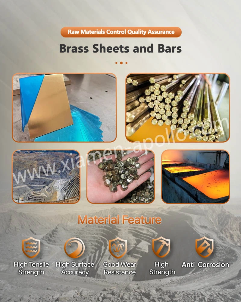
Machining Metallurgy: Pure Copper vs. Free-Machining Brass
C1100 Copper Conductivity and Machining Behavior
C1100 copper is widely selected where electrical conductivity is a primary design parameter. Its high copper content produces low electrical resistivity, but its ductility can create continuous chips and material adhesion at the cutting edge.
Typical machining controls include:
- C1100 copper: electrical conductivity commonly above 100% IACS depending on material condition
- Sharp carbide cutting edges with optimized rake geometry
- High-pressure coolant or directed coolant flow for chip removal
- Controlled cutting speed and feed rate to limit built‑up edge
- Tool wear monitoring before dimensional drift reaches the ±0.005 mm control limit
For switchgear terminals and current‑carrying CNC components, the machined surface should also be evaluated for burrs because residual burrs can interfere with assembly clearance, plating thickness, or electrical contact geometry.
H62/H65 Brass Cutting Stability and Chip Control
Brass such as H62 and H65 generally offers easier chip breaking and lower cutting resistance than commercially pure copper. This makes brass suitable for precision threaded components, terminal bodies, conductive spacers, connector components, and machined electrical hardware.
| Parameter | C1100 Copper | H62 Brass | Engineering Effect |
|---|---|---|---|
| Main characteristic | High conductivity | Better machinability | Determines cutting strategy |
| Typical conductivity | >100% IACS possible | Lower than pure copper | Select based on current path |
| Chip behavior | Long/ductile | Generally easy‑to‑break | Impacts process stability |
| Tool sticking risk | Higher | Lower | Requires proper tool geometry |
| Burr tendency | Moderate to high | Moderate | Needs deburring management |
| Typical application | Current‑carrying parts | Terminals, fittings, housings | Depends on electrical requirements |
For a copper CNC machining supplier, material certification should be linked to the production lot so the engineering team can distinguish machining variation from material‑property variation.
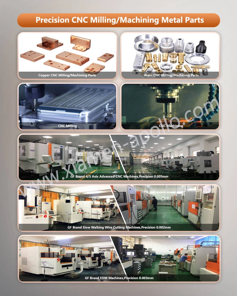
How ±0.005 mm CNC Tolerance Is Controlled During Electrical Part Production
A drawing tolerance of ±0.005 mm should not be treated as a machine specification alone. It is a process‑control requirement involving machine thermal stability, fixture repeatability, cutting‑tool condition, material batch consistency, measurement uncertainty, and inspection temperature.
For electrical components installed in switchgear or distribution equipment, critical dimensions commonly include terminal‑hole diameter, contact seating diameter, mounting location, slot width, thickness, and mating geometry.
±0.005 mm Dimensional Control Requires Process‑Level Monitoring
A stable CNC process should establish nominal dimensions, upper and lower limits, tool compensation values, and inspection frequency before volume production.
A typical control sequence includes: Material identification and incoming dimensional verification. First‑piece CNC inspection. Tool offset confirmation. In‑process dimensional measurement. Statistical monitoring of critical dimensions. Final CMM or calibrated gauge inspection. Batch traceability and inspection record retention.
For particularly tight features, the production environment should also control temperature because thermal expansion can become comparable to the permitted dimensional tolerance.
Ra 0.8–1.6 μm Surface Finish Supports Plating and Electrical Contact
Surface roughness is not simply a cosmetic parameter. It affects plating coverage, interface contact area, burr retention, cleaning effectiveness, and subsequent electrical contact resistance.
| Machining Requirement | Typical Engineering Target | Inspection Method |
|---|---|---|
| Dimensional tolerance | ±0.005 mm | CMM / calibrated gauge |
| General precision tolerance | ±0.01 mm | CMM / micrometer |
| Surface roughness | Ra 0.8–1.6 μm | Surface roughness tester |
| Edge burr | Controlled/removed | Visual + tactile inspection |
| Hole diameter | Drawing‑specific | Pin gauge / CMM |
| Flatness | Drawing‑specific | CMM / height gauge |
The final specification should always follow the component drawing rather than applying a generic tolerance to every feature.
Download Contact Material Spec Sheet
CNC Machining Versus Other Metal‑Forming Processes for Copper and Brass Parts
CNC machining is normally selected when electrical components contain complex profiles, controlled holes, internal threads, stepped diameters, slots, or three‑dimensional geometries that cannot be produced efficiently by simple stamping.
However, CNC machining removes material rather than forming it. For high‑volume conductive components with repeatable geometry, stamping, cold heading, or progressive die forming may offer a different material‑utilization profile.
CNC Machining and Progressive Stamping at ±0.005 mm Feature Control
| Factor | CNC Machining | Progressive Die Stamping |
|---|---|---|
| Material removal | Subtractive | Forming/shearing |
| Complex 3D geometry | Strong capability | Limited |
| High‑volume production | Suitable | Highly suitable |
| Tooling investment | Lower initial tooling | Higher die investment |
| Material utilization | Depends on geometry | Often higher |
| Tight local features | ±0.005 mm achievable on selected features | Depends on die design |
| Design changes | Relatively flexible | Die modification required |
| Typical materials | Copper, brass, aluminum, steel | Copper alloys, brass, steel |
For low‑to‑medium volumes, prototypes, replacement components, and geometrically complex electrical parts, CNC machining can reduce tooling dependency. For large‑volume flat terminals or stamped conductive components, progressive stamping may become more appropriate.
| Process | Dimensional Flexibility | Material Utilization | Production Rate | Typical Electrical Use |
|---|---|---|---|---|
| CNC turning | High | Moderate | Medium | Custom terminals |
| Cold heading | Moderate | High | High | Rivets, pins, conductive fasteners |
| Stamping | Moderate | High | Very high | Terminals, brackets |
| Milling | High | Lower | Medium | Complex copper blocks |
Process selection should be based on annual volume, geometry, tolerance, material cost, tooling budget, and downstream assembly requirements rather than machining speed alone.
Silver, Tin, and Nickel Plating Selection for Copper and Brass CNC Parts
Copper and brass surfaces can oxidize and form surface films that influence solderability, contact resistance, corrosion behavior, and interface stability. Plating is therefore selected according to the electrical interface, mechanical contact condition, environmental exposure, and assembly process.
The three commonly specified systems-silver, tin, and nickel-serve different engineering purposes.
Silver Plating for Low Contact Resistance and High Conductivity
Silver offers very high electrical conductivity and is frequently specified for mating electrical interfaces where low contact resistance is critical.
Typical design considerations include:
- Silver thickness specified in μm
- Base‑material surface preparation before plating
- Adhesion between plating layer and copper or brass substrate
- Surface cleanliness and contamination control
- Contact resistance after environmental testing
- Wear performance under repeated mating cycles
For electrical contacts, silver plating should not be specified only by nominal thickness. The engineering specification should define the minimum local thickness, measurement method, substrate condition, and acceptance criteria.
Tin Plating for Copper Electrical Terminals and Solderable Interfaces
Tin is commonly selected for copper and brass terminals where solderability, electrical conductivity, and cost control need to be balanced.
Tin‑plated CNC parts may be used in:
- Switchgear terminal assemblies
- Wire connection components
- Busbar interfaces
- Connector components
- Low‑voltage distribution equipment
The plating specification should define thickness, surface condition, substrate preparation, and applicable solderability or corrosion testing.
Nickel Plating for Surface Hardness and Environmental Protection
Nickel provides a harder surface than many soft conductive coatings and can function as a barrier layer between the substrate and an external coating.
For precision electrical CNC parts, nickel plating may be considered where the component requires:
- Higher surface hardness
- Wear resistance
- Barrier‑layer performance
- Improved corrosion resistance
- Controlled appearance and dimensional build‑up
Plating thickness must be included in the dimensional stack‑up because a coating on both sides of a feature can reduce hole diameter or increase external dimensions.
Consult Our Electrical Engineers Today
How Plating Thickness Changes Final CNC Dimensions and Contact Resistance
A plating layer is physically part of the finished component, so its thickness must be incorporated into the machining allowance and tolerance chain.
For example, if a cylindrical hole receives an internal coating, the final usable diameter decreases according to the coating thickness on both opposing surfaces.
For a simplified through‑hole calculation:
Final Hole Diameter ≈ Machined Hole Diameter − 2 × Coating Thickness
The actual result also depends on coating distribution, geometry, masking, current density, and plating process capability.
5–20 μm Plating Thickness Requires Dimensional Compensation
| Coating | Example Thickness Range | Primary Engineering Consideration |
|---|---|---|
| Silver | 5–20 μm | Conductivity/contact interface |
| Tin | 3–15 μm | Solderability / terminal connection |
| Nickel | 5–25 μm | Hardness/barrier protection |
These values are engineering examples rather than universal specifications. Final thickness should be established from the electrical, mechanical, environmental, and dimensional requirements of the component.
Contact Resistance Requires More Than Plating Thickness
Low contact resistance depends on several variables: Contact resistance = f(material, surface condition, contact force, geometry, oxide/film condition, plating, temperature)
A thicker coating does not automatically produce lower resistance. Surface cleanliness, contact pressure, interface geometry, coating composition, and substrate condition also affect the measured value.
For components used in low‑voltage electrical systems, the test method and measurement current should therefore be specified alongside the acceptance limit
FAQ: Precision CNC Copper and Brass Parts for Electrical Applications
How is silver plating thickness measured on CNC copper electrical parts?
Silver plating thickness can be measured using X‑ray fluorescence (XRF), metallographic cross‑section analysis, or other validated methods. The purchase specification should define the minimum thickness, measurement location, substrate, and acceptance criteria in μm.
What tolerance can a CNC supplier maintain on precision electrical copper parts?
Selected CNC features can be controlled to ±0.005 mm when machine stability, tooling, fixturing, thermal conditions, and inspection capability are properly controlled. The achievable tolerance depends on geometry, material, feature size, and production volume.
Can custom brass CNC parts be supplied with RoHS and REACH documentation?
Yes. Material certificates, RoHS declarations, REACH documentation, dimensional inspection reports, and plating records can be provided when specified in the purchase quality requirements. The documentation scope should be confirmed before mass production.

contact us
For drawings requiring Brass Multi Axis Machined Components with C1100 copper, H62/H65 brass, ±0.005 mm critical dimensions, controlled Ra surface finish, silver/tin/nickel plating, CMM inspection, RoHS/REACH documentation, or IATF 16949 process controls, submit the 2D drawing, 3D model, material grade, annual volume, plating specification, and critical dimensions for engineering review and production quotation.