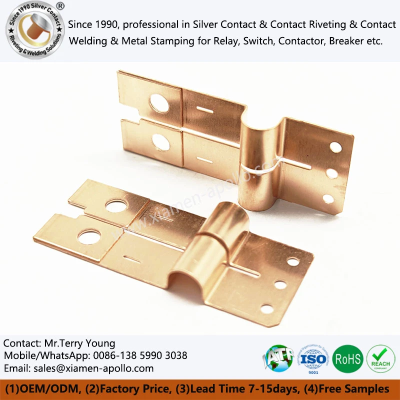
As electronic connectors continue to become smaller, more compact, and more demanding in electrical and mechanical performance, the material used for terminal components has become an important engineering consideration. Terminal Copper Beryllium Stamping Parts are used in connector terminals, spring contacts, sockets, pins, and other precision conductive components where strength, elasticity, conductivity, and dimensional stability must be considered together.
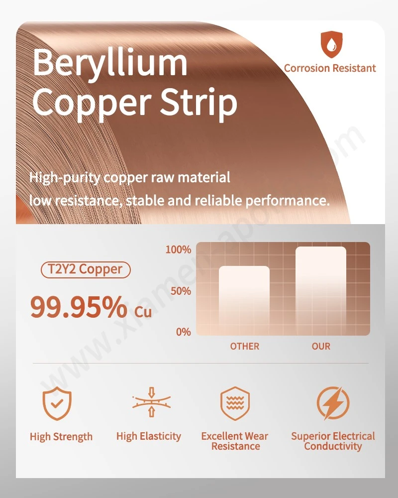
Copper beryllium is widely selected for applications that require a combination of mechanical strength and electrical conductivity. After appropriate heat treatment, the alloy can provide high hardness, elastic strength, and resistance to deformation while retaining useful electrical conductivity. These characteristics make it suitable for stamped terminal components that undergo repeated insertion, contact loading, or mechanical deflection.
Mechanical Requirements for Beryllium Copper Sheet Metal Stamping Parts
Connector terminals are subjected to mechanical loads during assembly and service. Insertion and withdrawal forces, contact pressure, vibration, and repeated deflection can gradually affect the dimensional stability of a terminal.
Copper beryllium alloys can achieve high strength through solution treatment and age hardening. Depending on alloy grade and material condition, certain grades can reach tensile strengths above 1,000 MPa, while hardness can increase substantially after aging.
For BeCu Copper Stamping Part for Socket Accessories, the required material condition should therefore be selected according to the terminal structure and working load rather than using a single strength value for every application.
Spring-type terminals also require sufficient elastic recovery. A properly selected copper beryllium grade can maintain contact force after repeated deformation, helping prevent excessive permanent set and loss of contact pressure.
Electrical Conductivity and Contact Resistance
Electrical conductivity is another major factor in terminal material selection. Copper beryllium does not provide the conductivity level of pure copper because the alloying elements and strengthening treatment reduce electrical conductivity. However, it offers a useful balance between conductivity and mechanical strength.
Depending on the alloy and temper, copper beryllium strip can provide conductivity within a range suitable for various connector applications. Material selection should consider the required current, contact resistance, temperature rise, and mechanical loading at the same time.
For Beryllium Copper Stamping Parts, low and stable contact resistance depends not only on the base material. Contact geometry, normal force, surface finish, plating, contact area, and assembly conditions can all affect electrical performance.
Stamping Formability and Terminal Geometry
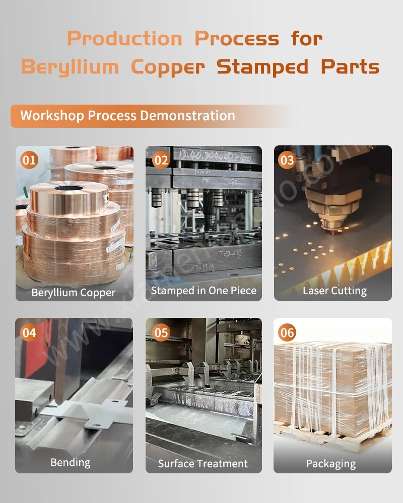
Copper beryllium strip can be processed by precision stamping to produce terminals with bends, slots, contact beams, locking features, mounting sections, and other functional geometries.
The material condition has a direct influence on stamping behavior. Annealed or suitably conditioned strip can provide better forming capability, while precipitation-hardened material provides higher strength but may require greater forming force.
For complex Beryllium Sheet Stamping Terminal Parts, the stamping process should therefore be considered together with material hardness, strip thickness, bend radius, forming direction, and dimensional tolerance.
Typical terminal structures may include:
- Spring contact beams
- Connector terminal pins
- Socket contacts
- Retention clips
- Crimping terminals
- Shielding and grounding contacts
- Precision electrical terminals
The design of the stamping die also affects burr formation, dimensional consistency, bend accuracy, and surface condition.
Dimensional Accuracy and Quality Control
Connector terminals operate within relatively small assembly spaces. Even minor dimensional deviations can affect insertion force, contact position, retention, or mating performance.
For this reason, the production of Beryllium Copper Sheet Metal Stamping Parts for Electronics requires control of material thickness, flatness, hole position, bend angle, terminal width, contact height, and other critical dimensions.
Typical quality-control procedures may include dimensional inspection, material verification, hardness testing, electrical conductivity testing, surface inspection, and sampling of critical stamping dimensions.
For high-volume connector production, progressive stamping can provide consistent production of complex terminal geometries. Process capability should be evaluated against the actual drawing tolerances rather than relying only on nominal machine accuracy.
Surface Treatment and Corrosion Resistance
The operating environment of a connector can influence the required surface treatment. Copper beryllium has useful corrosion resistance, but exposed terminal surfaces may require additional protection depending on humidity, temperature, electrical requirements, and mating conditions.
Common surface treatments for connector terminals include nickel, tin, silver, and gold plating. The selected coating influences electrical contact behavior, wear resistance, corrosion protection, and solderability.
For example, plating may be applied selectively to the contact area or soldering area rather than covering the entire Beryllium Copper Strips for Stamping Parts. This approach can reduce material consumption while maintaining the required surface properties at functional locations.
Thermal and Environmental Considerations
Connector terminals may operate under continuous current, cyclic loading, elevated temperature, vibration, or corrosive atmospheric conditions. These conditions can affect contact force, resistance, oxidation, and long-term dimensional stability.
Copper beryllium retains useful mechanical properties at elevated temperatures, but the actual operating temperature limit of a stamped terminal depends on the alloy grade, temper, plating system, electrical load, contact resistance, and connector design.
Therefore, temperature performance should be evaluated at the complete component or connector level rather than assigning a universal operating temperature to all copper beryllium terminals.
Application Areas of Stamping Beryllium Copper Forming Parts Copper
Beryllium Copper Terminals Made by Stampings are used where electrical conductivity must be combined with spring characteristics and mechanical stability. Typical applications include automotive connectors, industrial control connectors, telecommunications equipment, electronic devices, test sockets, and high-cycle electrical interfaces.
As connector designs continue to reduce terminal size while increasing contact density, material selection and stamping process control become increasingly important. The combination of alloy properties, stamping accuracy, heat treatment, and surface treatment directly affects the functional behavior of the finished terminal.

Conclusion
Terminal Copper Beryllium Stamping Parts require more than a material with high strength and conductivity. Their performance depends on the interaction between alloy grade, temper, stamping geometry, dimensional tolerance, surface treatment, contact design, and operating conditions.
For connector applications, copper beryllium provides a useful combination of mechanical strength, elastic recovery, electrical conductivity, and stamping capability. Proper material selection and process control are therefore essential when developing precision stamped terminals for repeated mating, compact connector structures, and demanding electrical interfaces.
contact us